
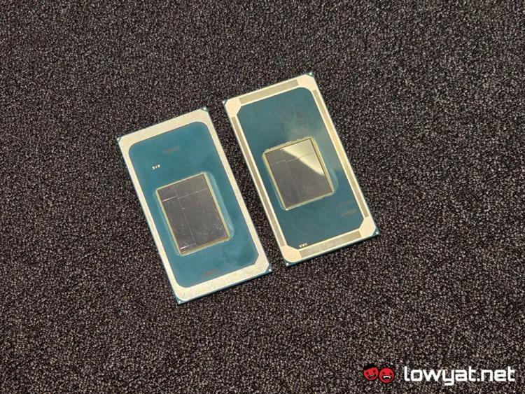
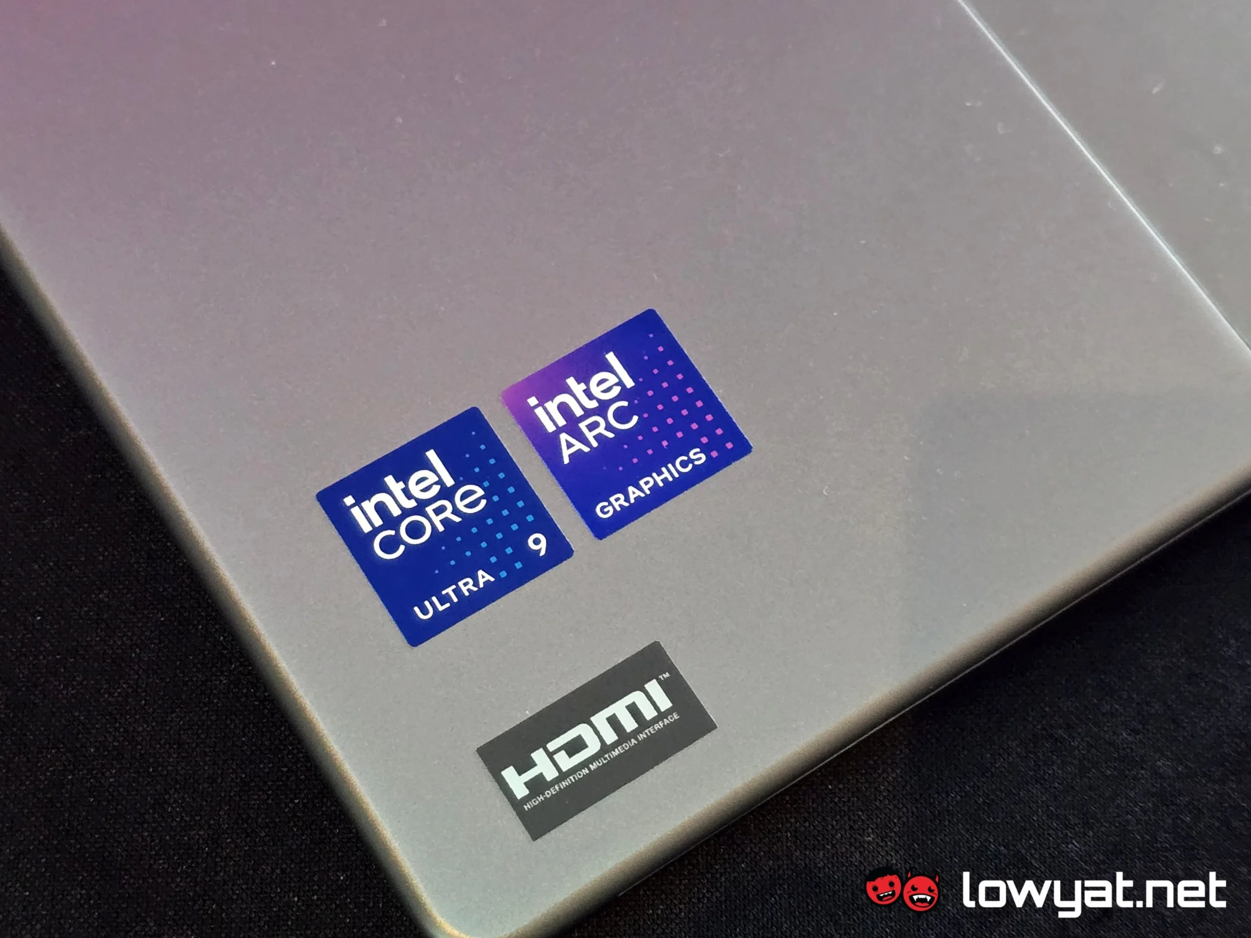
Intel, and more specifically, Intel Foundry, became one of the first companies in the world to enter high-volume manufacturing, a subset of its Panther Lake Core Ultra 3 Series of processors. The subset of processors was manufactured using ASML’s High NA extreme ultraviolet (EUV) lithography technology.
Why Is This Important?
The achievement serves as a milestone and feather in Intel’s cap, as it confirms the operational capacity of the chipmaker’s Foundry, which is now qualified to run High NA EUV layers on its 18A process node, at its fab in Oregon. Panther Lake is the first chipset and architecture to be based on the 18A process node, so it makes sense that the company would want to take full advantage of the technology.
High NA EUV, by the by, has long been considered as the successor to current EUV technology, with the promise of enabling fabs to print smaller, denser circuit patterns that are becoming increasingly difficult to cut with existing tools. ASML and its High NA EUV builds on the same 13.5nm EUV, used in many of today’s scanners, but increases the optical system’s numerical aperture (NA) from 0.33 to 0.55. For context, NA is the unit of measurement of the amount of light a lens system can collect and focus on a single wafer.
More importantly, being able to run high-volume manufacturing means that Intel wouldn’t have to rely on complex multi-patterning techniques, and in this case, the simplifying of manufacturing and improved feature fidelity can be done in-house, rather than having it outsourced.
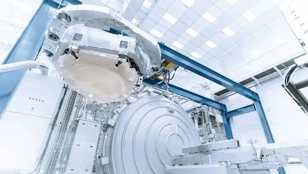
“With increased resolution and better process control, the introduction of High NA EUV marks a substantial development in semiconductor lithography,” said Christophe Fouquet, ASML President and CEO. “We are proud to play a role in enabling the smaller, denser patterning that will accelerate advancements in AI and other emerging technologies.”
(Source: ASML, Tom’s Hardware)
