
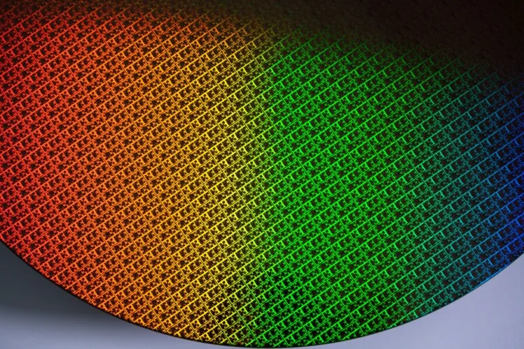
It seems like Intel has solved its issues with its latest 18A process node. The blue chipmaker has reportedly managed to solve its yield issues and has already entered into stable high-volume production phase.
According to the sell-side equity research firm, BlueFin Research Partners, Intel appears to have fixed the yield issues that plagued it. As such, having shifted to a stable production line is nothing short of a milestone for the company. To get a little technical, the defect density typically falls within the D0=0.1 to D0=0.2 range, suggesting Intel reached that range after several months of volume manufacturing.
To be clear, 18A has already launched; Panther Lake is the first architecture to be built around the die lithography. Again, this just means that the chipmaker can ramp up production of the chip.
As of now, 18A production is concentrated at two facilities: Fab 52 in Phoenix, Arizona, and another fab in Hillsboro, Oregon. Together, they produce about 30,000 wafers per month. That output is currently sufficient to meet Intel’s internal demand, including Panther Lake production, but the company will need to expand capacity as more products transition to 18A.

Adding on to the good news, Intel has also started risk production of 18A-P over at its D1X site in Oregon. This process node is basically a forked evolution of the 18A process, and is slated to move to Fab 62 once it is fully qualified for long-term, high volume manufacturing. As per its roadmap, the blue chipmaker will move on to its next generation 14A process node.
For now, Intel will be focusing mainly on 18A and 18A-P.
