
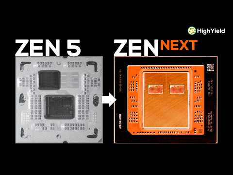
AMD’s upcoming Zen 6 CPU architecture is reportedly poised to offer significant improvements, both in power efficiency and latency improvements. All from the adoption of a new chiplet design.
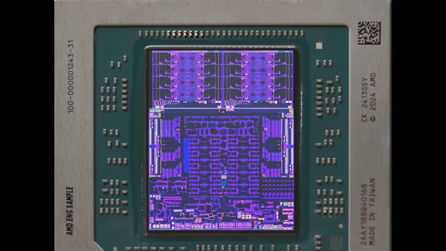
According to YouTuber High Yield, this new CPU design was first shown in Strix Halo APUs, in which AMD uses an architectural design called SERDES PHYs. To put it simply, the chip design essentially brings the Core Complex Die (CCD) edges right up to each other on the PCB, virtually leaving little if no gap between them.
Right on top of these Zen6 CCDs are high-speed serial lanes, used to facilitate communication between each die and through the substrates beneath them.
SERDES PHYs is, in layman terms, a serialiser and deserialiser. It is by no means a new technology, with AMD having used it since Zen 2. The way it works is as per TweakTown’s explanation:
Data from the CPU cores is serialized into high-speed bitstreams, sent across the substrate, and then deserialized again on the other side. While this technique has worked well since Zen 2, it has two major downsides: it consumes extra power because the hardware has to encode/decode, clock recovery, and latency, as the data needs to be converted back and forth.
Another point to note is that, unlike previous generation chips, Strix Halo-based processors don’t use AMD’s Infinity Fabric between the CCDs. In fact, the dies actually use a far denser and much more parallel connection that skips the serialisation step usually required for Infinity Fabric.
You can check out High Yield’s video to better understand their reasoning for Zen 6.
(Source: High Yield via YouTube, Hot Hardware, TweakTown)