
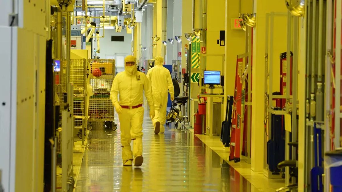
Intel says that its upcoming 14A manufacturing technology – assuming it hasn’t abandoned it by the time of production – will be more expensive than its 18A product node. This is reportedly due to the blue chipmaker using ASML’s next generation Twinscan EXE:5200 High-NA lithography machine, with a 0.55 numerical aperture optics.
“14A is more expensive than 18A,” David Zinsner, CFO at Intel, told an audience at the Citi 2025 Global TMT Conference. “It is not significantly more expensive in terms of investment. But it is a higher wafer cost, for sure and partly that is because we are expecting to use High-NA EUV tools in 14A, which was not the case in 18A.”
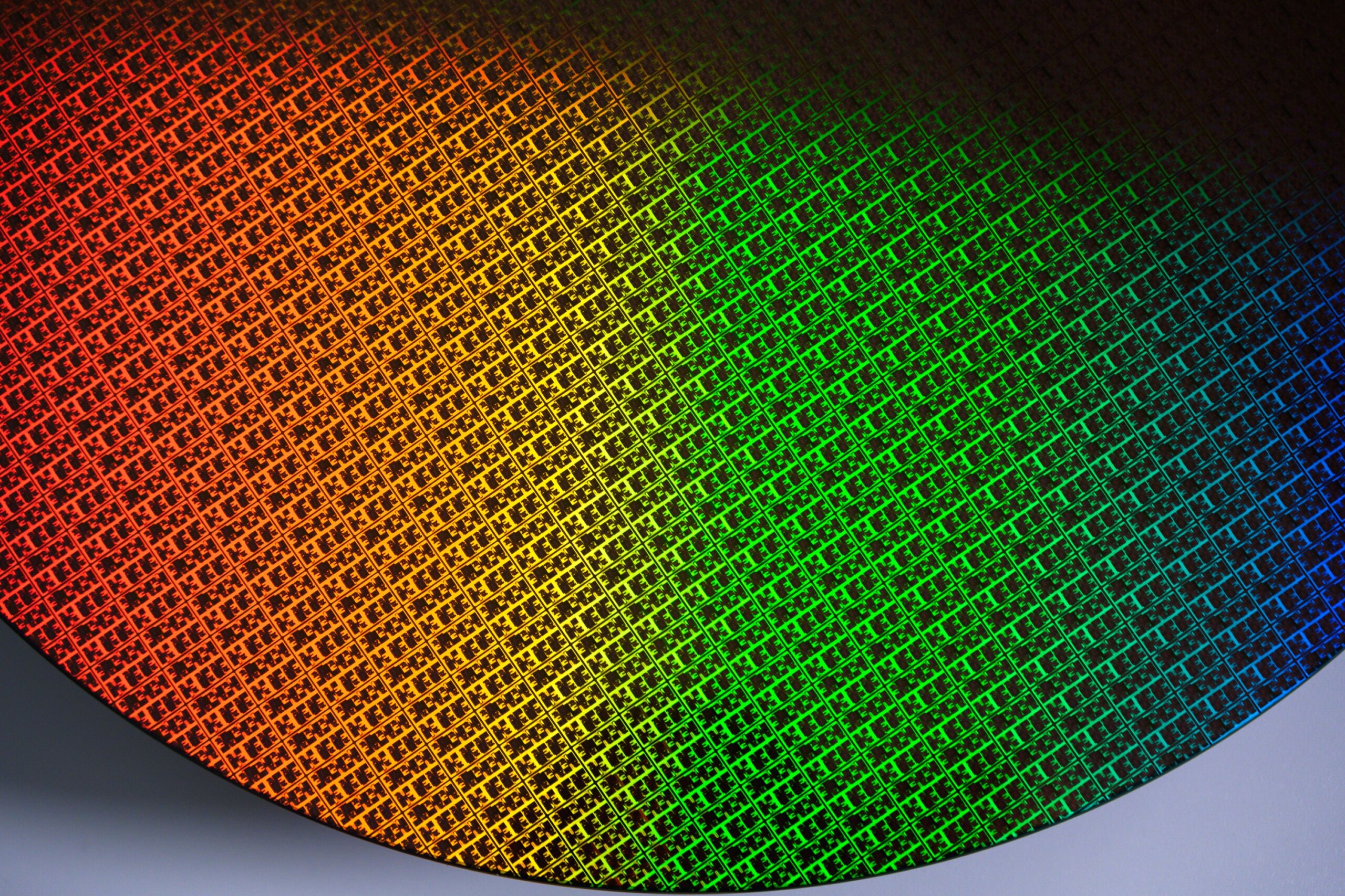
ASML’s Twinscane EXE High-NA EUV systems can achieve an 8nm resolution in a single exposure, which is a significant jump from the 13.5nm resolution of current low-NA EUV tools. Mind you, they can achieve the same 8nm resolution but only via double patterning, which is more complicated in its process and has a higher rate of error in yields.
With High-NA EUV machines, that rate of error is slashed by about 50%, which is also why these machines are more expensive. For context, the EXE:5200B tools are expected to cost US$380 million (~RM1.6 billion) a pop, compared to the current Low NA EUV Twinscann NXE:3800E that costs US$235 milion (~RM989 million) per unit.
Intel reckons that with ASML’s new systems, its 14A fabrication process should be able to offer between 15% and 20% better performance-per-watt over 18A, or a reduction of up to 35% in power consumption. Specs-wise, 14A will be made using the new RibbonFET 2 manufacturing process, which is an upgraded Gate-All-Around (GAA) transistor structure, along with PowerDirect, which is a backside power delivery network that connects components directly to transistors.
(Source: Tom’s Hardware)