
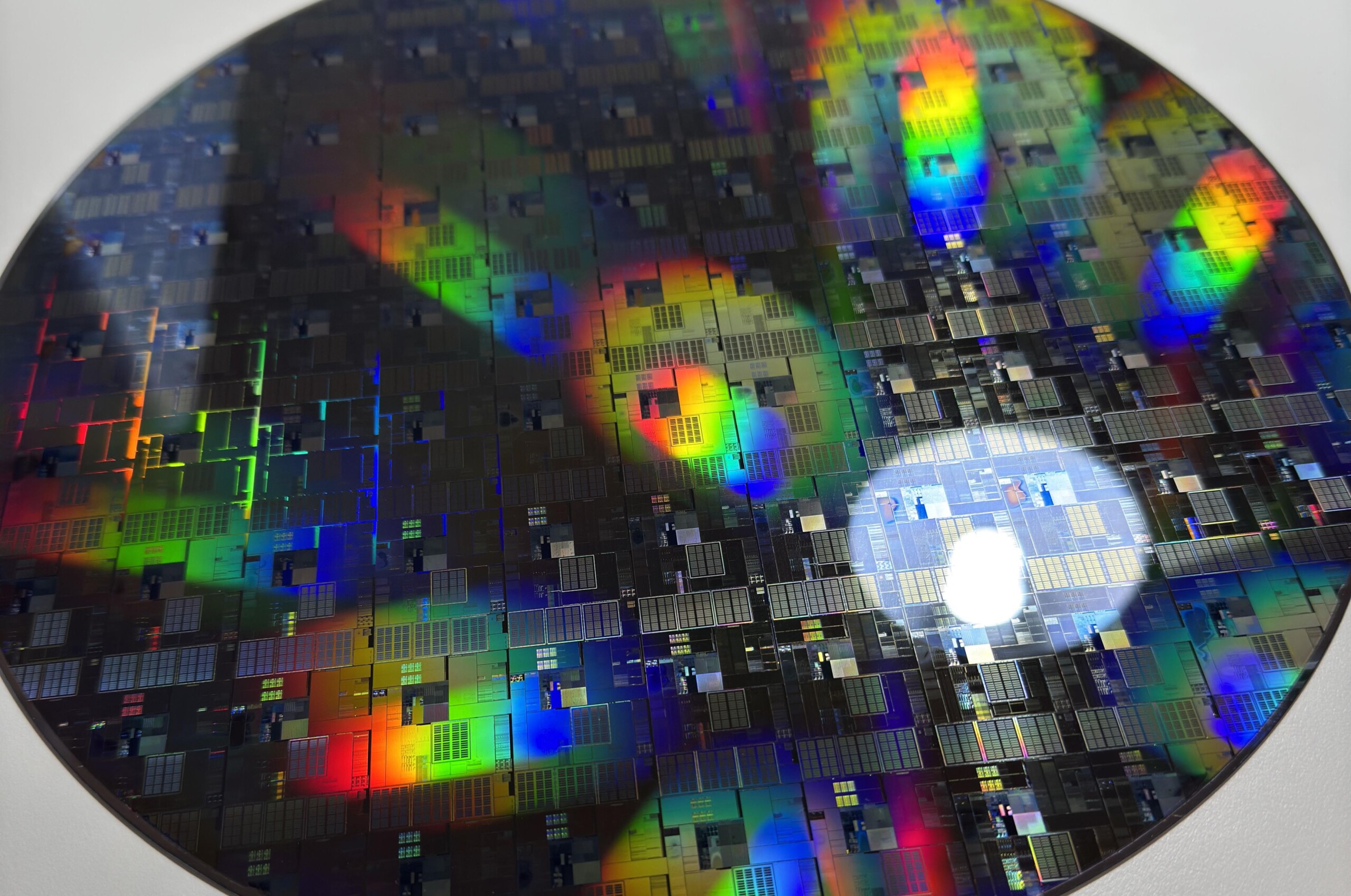
Some dumpster diver in China lucked out when they went scavenging inside TSMC’s garbage recently and found a literal Chip Wafer inside a rubbish bin outside one of its factory in the city of Nanjing. The water was found in all its uncut glory, and is rallying jokes about the fab taking “chip binning” a little too literally.
Images of the chip wafer was posted on Reddit by the Redditor AVX512-VNNI, who found it fully intact. A bit more digging also revealed that the TSMC wafer was a 12nm silicon. Not the most advanced fab the Taiwanese company but hey, it’s still up there.
Found this in a dumpster near TSMC fab, how to cut this into usable GPU?
byu/AVX512-VNNI inpcmasterrace
AVX512-VNNI had also asked Reddit candidly if anyone had the know-how to cut up the wafer into individual chips. It’s a candid question simply because the wafer doesn’t contain any chip design. Basically, the unit that was dumped out was simply a test wafer containing dummy circuitry layouts, meaning that TSMC was likely using the tossed-out component to make some calibrations and for a more complex and advanced lithography machine.
All in all, the discovery of the tossed out chip wafer wouldn’t be considered a security risk but that shouldn’t detract from the fact that its discovery was something refreshing, if not fun.